This is a list of my most used keyboard shortcuts and actions in Altium Designer. Coming from a much simpler software such as Eagle CAD, some of them took me a while to figure out. I will keep updating this post periodically with new stuff.
Keyboard shortcuts (PCB)
- J , L : Jump to location, press intro after introducing the coordinates.
- Q : Switch between mm/inches.
- Ctrl + M : Measure distance between two points.
- 2 / 3 : Switch board view to 2D/3D mode.
- G : Pop up Snap Grid menu.
- Ctrl + Click on a net : Select everything connected to that net.
- Tab : Pop up properties dialog of the placing component/routing line.
- Space / Shift + Space : Rotate components and cycle through routing options.
- Shift + R : Cycle routing modes (ignore, avoid or push obstacle).
- + / - : Switch to previous/next layer when routing.
- M , C : Select a component from the list to move it.
- L : Flip component.
- Ctrl + Shift + Left Click : Set current mouse position as the dx,dy center.
- Ctrl + Mouse wheel : Zoom in/out.
- Shift + Hold Right Click : Move to rotate board in 3D view.
PCB Layout tips
Add/change via tenting properties for all vias:
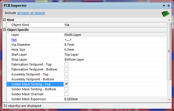
Pick one via, right click on it and select Find Similar Objects…. Click [OK] and the PCB Inspector window will pop up. From this panel you can change massively the properties of all vias, that are already selected. For via tenting, click on the Solder Mask Tenting checkbox.
Create a PCB board shape
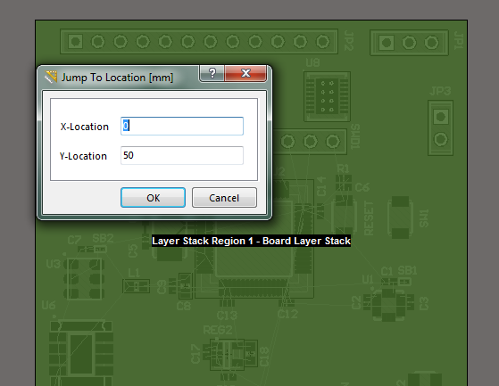
Switch view mode to Board Planning mode by clicking on shortcut 1. Click on menu Design > Edit Board Shape to change the size of the board moving the border handles. To define an exact shape, click on Design > Redesign Board Shape and set the vertices using the J , L jump to location shortcut. If the board is not correctly centred, click on Edit > Origin > Set to set the centre.
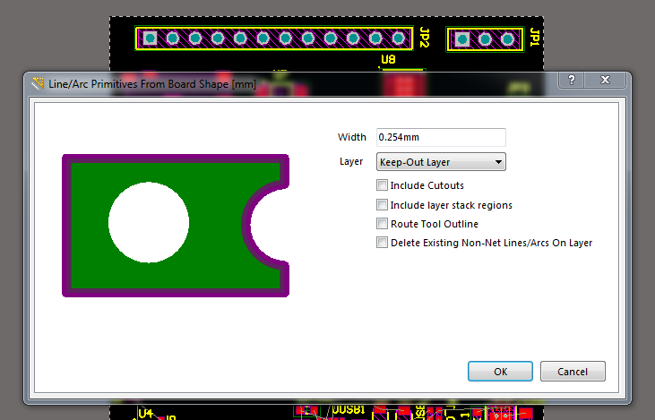
After this, change view mode back to 2D Layout Mode (click on 2) and click on menu Design > Board Shape > Create Primitives From Board Shape. Select the options that suit your design and click OK. A contour will be created in the layer that you have selected (Keep-out layer by default).
Later on when the board is finished and when you are configuring the options for gerber files generation, select this layer as the board outline.
Put a logo in the PCB and move it around:
Be aware that for this to work you will need a black and white well defined image.
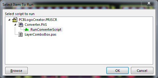
First, download the Altium Example Scripts and extract it.
Click on the menu DXP > Run Script … and a select window will pop up. Click on the [Browse] button and navigate where we extracted the example scripts. Open Scripts\Delphiscript Scripts\PCB\PCB Logo Creator\PCBLogoCreator.PRJSCR, select RunConverterScript and click [OK].
Click on [Load] and select the image. Change the board layer to Top Overlay. Play with the scaling factor to get the correct size of the logo.
![]()
Click on [Convert], and when it is finished click on [Exit]. A new board tab will be open in the background with the logo rendered.
To be able to move the logo around easily, you need to join all the segments in one block. Select the full logo with left click + dragging. Right click on the selection and click on Unions > Create Union from selected objects
![]()
Now, to copy the logo to your board, right click on the logo, Copy, and click on the logo again. After this, go to the your board tab and right click, Paste. Since the logo is already a block, you will be able to freely click on it and drag it around.
![]()
Add multiple boards to a PCB Panel:
Create a new PCB Project with the menu File > New > Project > PCB Project. Add a new PCB document to this project, open it and click on the menu Place > Board Embedded Board Array/Panelize. Select the PCB Document to add and the number of units in Column/Row Count.
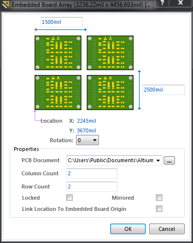
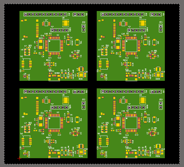
Different PCBs can be placed in the same panel. The panel and the rest of the PCBs need to be open when modifying the PCBs, so the PCB panel is updated automatically.
Show GND/VCC net connections and pads in different colors:
Select Nets in the dropdown menu on the PCB left side panel. Click on <All Nets> and search down for the net.
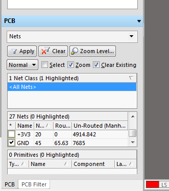
Select the checkbox and doble-click in the label. A menu will pop up that would allow us to change the Connection Color
Thank you that is very useful.